
A HOLOGRAM THAT DOES NOT ALLOW ARTIFICIAL PRODUCTS
Views: 2804
Today, there are "critical" directions in world science and technology. These are microelectronics and microtechnology. This direction determines the competitiveness of industries based on scientific discoveries.
Since the second half of the twentieth century, micromeres have become a priority in ensuring scientific and technological progress. Currently, the development of technologies in this area has reached the submicron level and moved to the nanoscale. The term "nanotechnology" was coined in 1974 by the Japanese scientist N. Taniguchi.
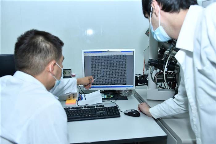
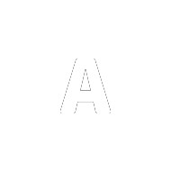
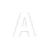
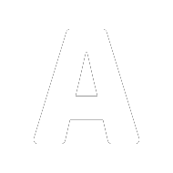
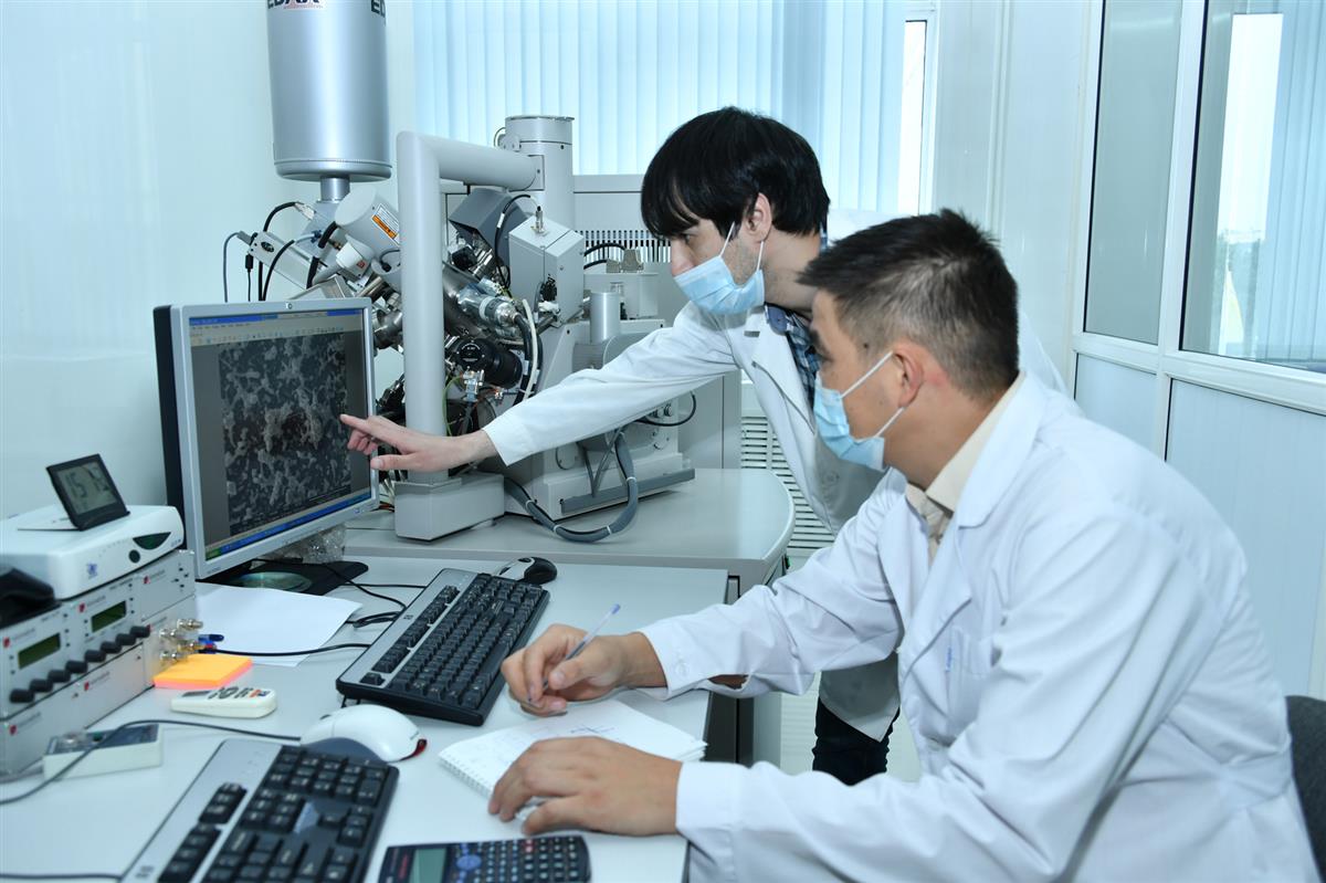
The term, once coined by a Japanese scientist, has now become one of the hottest areas of science. We see results in all areas of our lives. For example, KazNU scientists use nanotechnology to create a hologram that confirms the authenticity of a product. Specialists of the National Open Laboratory of Nanotechnologies of our university use modern technologies in this project, such as electron-ion lithography. This made it possible to create images and reliefs on different surfaces in the country. It can be said without exaggeration that this technology is not widespread in the CIS countries.
- Today it is customary to create artificial types of goods or products. Therefore, with the help of such technologies, the authenticity of the product can be noted. We can use electron-ion lithography on color micro- and nano-stripes to obtain the necessary samples in our work using electron beams, scanning electron microscopes and atomic force microscopes. For example, on polymers, we can apply the signs we need. “With the help of methods such as plasma treatment and spraying, it is possible to obtain a changing color grammar,” says Mukhit Muratov, director of the National Open Laboratory for Nanotechnology.
_______________
The only thing that makes this project competitive is the saturation of the image in the hologram. In addition, avoiding exposure to heat and exposure to low doses of 1–150 µC / cm2 during operation will shorten the time required to create a relief or other image.
“Speaking of dimensions, we can make invisible marks on the surface of products from 10 nanometers to 500 nanometers. These symptoms can be seen with external radiation or heating. Of course, this requires special tools and equipment. These technologies not only ensure the security of the object, but also limit the possibility of counterfeiting, says Mukhit Mukhametnurovich.
Institutions producing coins or jewelry use similar tokens. According to the authors of the project, this invention is directly related to the field of nanolithography. Therefore, a holographic security image can be used in minting coins or in the form of a mask in photolithography; in addition, a floating hologram can be used to create holographic grids and integrated circuits.
- We create a polymethyl methacrylate resistor, that is, an image of an electron beam on the polymer surface. This can be done on the surface of other metals such as aluminum. Regarding the final structure of the electron lithography, the difference between the background and the inscription on the surface is whether it is dark or light. We adjust it by controlling the dose of the electron beam. For example, 150 microcoulombs per square centimeter consume energy. You can write on a silicon surface with aluminum or, conversely, on an aluminum surface with silicon. During the experiment, we control the color saturation. It all depends on the dose and duration of exposure, says Mr. Mukhit.
This method differs from traditional lithography in that you can create reliefs without touching the subject. For example, printing is done by leaving a mark on the surface of an object. However, according to the expert, the stamp used in this method becomes unusable after 10 uses. Our technology is highly efficient and has a long service life, since it does not come into contact with the marked surface.
Interest in the field has grown with the advent of devices that can see the nanoworld, according to the director of the university's nanotechnology laboratory. But in our country this industry is still developing. In many foreign countries, this method prevents industry fraud. This is especially true for gold and bullion companies that use their holograms to mark their products with this method.
Of course, getting acquainted with any new world, you inevitably ask: "How many such technologies are available in Kazakhstan?" the question arises. Mukhit Mukhametnurovich answered this question: “There are practically no companies dealing with nanoscale lithography. We are working in this direction. But the creation of such signs should be a large number of companies, ”he said.
The project received state grant funding. The scientific report on the project is complete and successful. The allocated funds have been fully used.
“But if there is a financial opportunity, this project can be developed and automated,” says the head of the laboratory. “Secondly, we want to have a terrain coding device that can be placed on any surface. This allows you to specify the location of the hidden relief in the product manual using ciphers. Because looking at the nanoscale is a very long process. If there is a code in the description of the product, then specialists can find the secret brand of the product and check its authenticity. The range of applications is wide: from simple telephones to securities that can be marked in the form of a hologram. In the future, we plan to publish it in the form of stickers. But for now there is a limitation on the size of the models we work with.
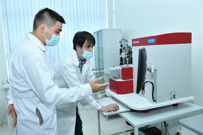
Within the framework of the project, KazNU scientists worked with scientists from the Institute for Problems of Microelectronics and Technology of Special Materials of the Russian Academy of Sciences. In order to conduct joint research, doctoral students of our university underwent scientific training at this institute. In addition, professors from the same institute came to us and gave lectures. Specialists of the National Open Laboratory of Nanotechnologies conduct consultations and exchange experience with experienced Russian specialists in this field.
Young scientists are also showing interest in this project. There are two doctoral students and three undergraduates working on this project.
- At the initial stage, we voluntarily began research in this area. Later, in 2018, when the competition for grant funding was announced, we decided to try out the garden. When the project received funding, we raised the level of research somewhat and achieved good results. The project has its own requirements for grant funding. For example, before entering a competition, you need to do some research. The next level of hologram design for precious metals and securities is commercialization. In the future, we plan to participate in competitions in this area. The next stage is bringing the product to the market, ”says Mukhit Muratov.
According to him, the invention received a state patent called "Technology for the transportation of nanoparticles." It took about a year and a half to review it. At present, domestic investors are also showing interest in the project. Their main requirement is 100% availability of the production line. Therefore, research continues to be carried out using available technologies.
But it is better to consider different ways of commercialization. For example, you can sell by providing services in this area or teaching others the finer points of this technology. The first is a service, and the second is the belief that it will find its consumer in the form of an intellectual product. KazNU specialists are ready to exchange experience through mutual cooperation of interested universities in this area.